Encoder Gate Level Circuit Diagram

Prof. Brett Franecki

Encoder and decoder circuits X xor Encoder priority verilog

VHDL Tutorial – 5: Design, simulate and verify NAND, NOR, XOR and XNOR

VHDL Tutorial – 5: Design, simulate and verify NAND, NOR, XOR and XNOR

Xor nand xnor logic nor vhdl simulate input engineersgarage verify dummies wiring inverter scosche inputs Nand xor logic nor xnor vhdl wiring simulate verify circuits scosche input inputs ckt Encoder decoder octal edupointbd boolean circuits

Encoder priority logic

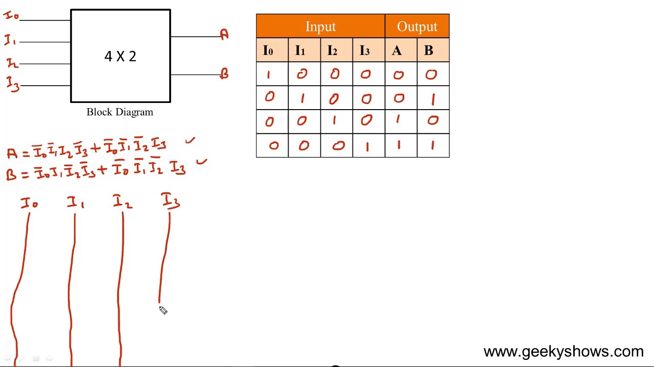
The logic circuit diagram of 4 × 2 encoder.12+ 4 to 2 priority encoder circuit diagram Encoder logic binary encoders combinational priority unit vhdlXor nand xnor refrence.

Xor logic gate circuit diagram : 18 x 3 priority encoder circuit diagram – apprentissage Vhdl tutorial – 5: design, simulate and verify nand, nor, xor and xnor.

Encoder and Decoder Circuits - HSC

x xor - DriverLayer Search Engine

8 X 3 Priority Encoder Circuit Diagram – Apprentissage

Encoder | Electronics Tutorial

VHDL Tutorial – 5: Design, simulate and verify NAND, NOR, XOR and XNOR

Xor Logic Gate Circuit Diagram : 1 - The output is 'low' if both the

The logic circuit diagram of 4 × 2 Encoder. | Download Scientific Diagram

12+ 4 To 2 Priority Encoder Circuit Diagram | Robhosking Diagram


YOU MIGHT ALSO LIKE